Turing Tumble Community

Attempt to build a CPU by limiting the individual gear bit chain to a maximum of 8 parts

The other day, I built an MCPU, a small but standard CPU with arithmetic and jump instructions.

That time, however, I used a gear bit chain consisting of a large number of parts in each block, specifically dozens of parts.

That may be fine for theoretical calculations, but when we consider the actual assembly of the parts, the practical gear bit chain would be about 10 parts due to friction and rattling.

Therefore, I thought about reducing the number of parts in the gear bit chain, and as a result, I was able to build it with a maximum of 8 parts.

In the beginning, each block is described.
The parts are described as follows.
notation

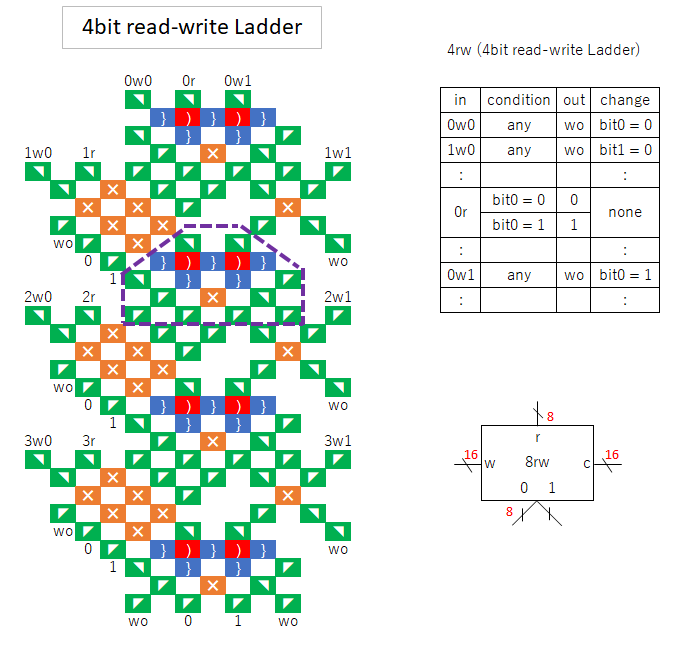
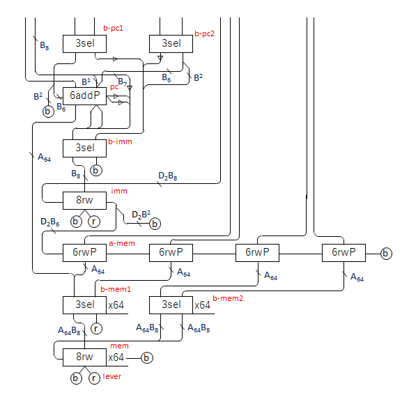
“rw” is a block that has read-write functionality.
31
Arrange the gear bit chains, which are independent of each other, according to the number of bits.
In the example of how to assemble the parts, I wrote with 4 bits, but in reality, 8 bits are used.

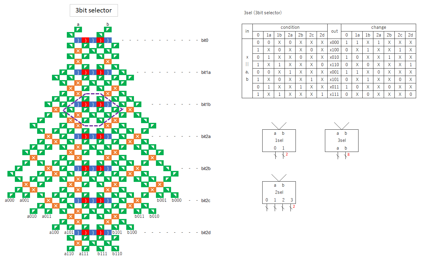
“rwP” is similar to “rw”, but branches depending on the bit when reading.
34
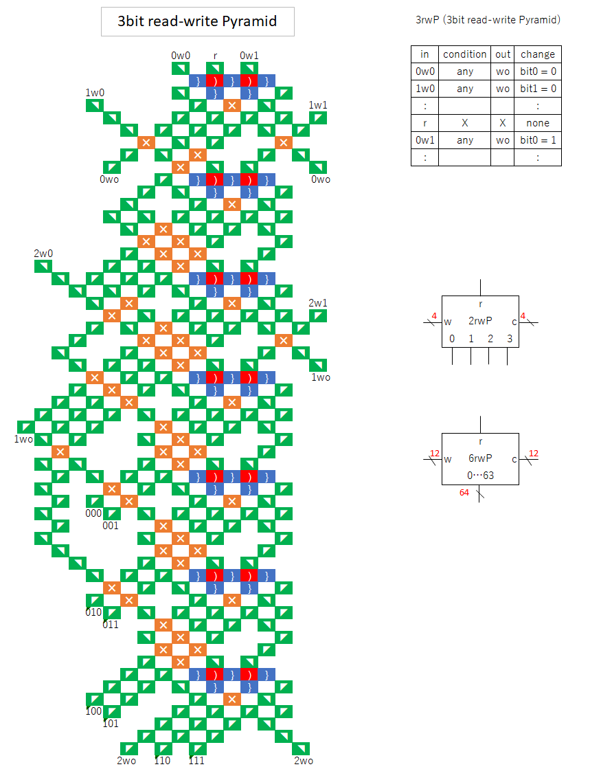
To achieve this function, the number of gear bit chains is 2^bit-1.
For example, if it is 2 bits, there are gear bit chains a and b corresponding to bit 2.
When writing, the same bit is written to a and b.
When reading, if bit1 is 0, it goes to a, if it is 1, it goes to b, and so on, following the tournament table in reverse order.
When building a CPU, either a 2-bit one or a 6-bit one is used.

“add” is a block with an additive function.
32
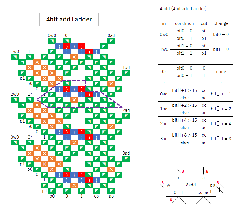
It is similar to “rw”, but instead of writing 1, it adds according to the bit.
Because of the carry, the input of +1 comes from one of the two outputs with or without carry, regardless of the bit.
In CPUs, 8-bit ones are used for addition instructions.

“addP” is a bitwise branch of “add”.
35
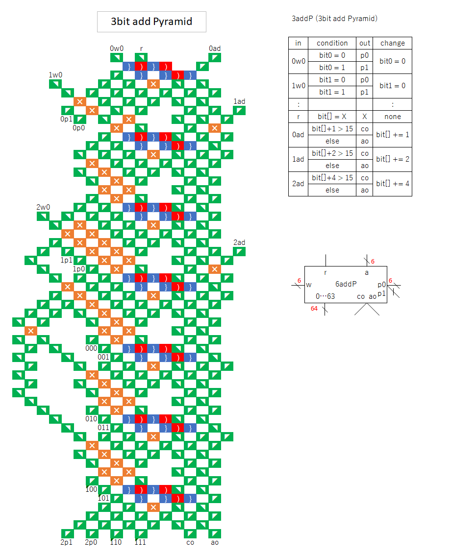
Use a 6-bit program counter, and select the one with the specified address from 2^6 memories.

“sel” is output to the corresponding exit depending on the input order, like a counter.
33
However, there are two input systems, both of which change the same counter.
For example, it corresponds to bits 0 and 1, and the operation is performed so that the digits do not deviate for either input.
The 1-bit sel is used for the top and bottom, the 2-bit for the phase, and the 3-bit for the bit-specified sequence.

“scc” is an extension of “rw” and has two w0 systems.
36
It is 1 bit, and only w0’ can read the previous information.
1scc means 1bit-set-clear-clear.
BitA and bitB in this module is same.
Used for flags in the CPU.
Flags need to be cleared by jmp and add, but this mechanism is necessary because they need to go a different route.
It has two clear inputs (write 0), one for clearing addition and the other for clearing JMP.

Based on the above blocks, the CPU was constructed as follows.

01

02

The initial condition of the chart is that only the memory has a value in it and the others are 0.

The first ball is shown in action.

[1sel]
Because of the order of top, we go to the left root. d2 indicates that there are two lines, (b) and (r).
The downward triangle means that the two are merged.
[3sel]
It branches into 8 lines depending on the bit.
[2sel]
Corresponding phase.
It enters the unit of the corresponding bit from eight.
Therefore, OUT will also be eight, but it will be integrated in this route.
[6addP]
It is divided into 64 lines according to the memory address.
[3sel]
Of the 64 units, it goes into the one corresponding to the address.
There are 8 outputs for each bit, so the total number of paths is 64x8.
[8rw]
It is input to the corresponding bit of the unit at the corresponding address.
The memory of that location is read to determine the next ball.

Second ball

[1sel]
The route to the right will be chosen.
[3sel]
[2sel]
Take the leftmost route.
[8rw]
There are 16 of them, although they are omitted in the figure.
There are two line inputs for each bit, and 0 or 1 is written.
The output branches at B^2 and B_6.
B^2 is the upper 2 bits, meaning {6…7}.
B_6 is the lower 6 bits, meaning {0…5}, which corresponds to the address.
[6rwP]
Write the lower 6 bits to allow for address branching.
Since bottom is a write, not read, the next balls will all be blue.

The third ball is almost the same as the first ball, but the bit corresponding to each [3sel] unit takes a different route.
After that, it proceed in the same way, and on the 2×8+1=17th ball, the [2sel] of PHASE moves to the second.
It takes 2×8×4=64 balls to complete the cycle. This is equivalent to one line of the assembly program.

The matrix for this operation is as follows.

11

12

The column starting from the leftmost “X” corresponds to the first ball.
For the first ball, top/btm is 0 and phase is also 0.
Whether the ball is “X”, i.e. blue or red, first change the state of [1sel] in top/btm from 0 to 1.
Then, enter bit 1.

Here, the route is split according to the bit ★ of the memory.
At the same time, the memory of bit 1 is rewritten to ★+1.
In phase 1, we enter the [2sel] corresponding to ★, and perform branching and rewriting.
After this, for the sake of the route, the ★ will be merged.
In addition, it branches according to the address ◆ of the memory in [6addP] of pc.

In addition, it goes through [3sel] prepared for the number of addresses, and branches to ★’ depending on the bit.
Note that ★’ is the same as ★.
After branching to a total of 512 addresses (64 addresses and 8 bits), it enters the corresponding bit of the corresponding mem unit [8rw].
The value :heart: 
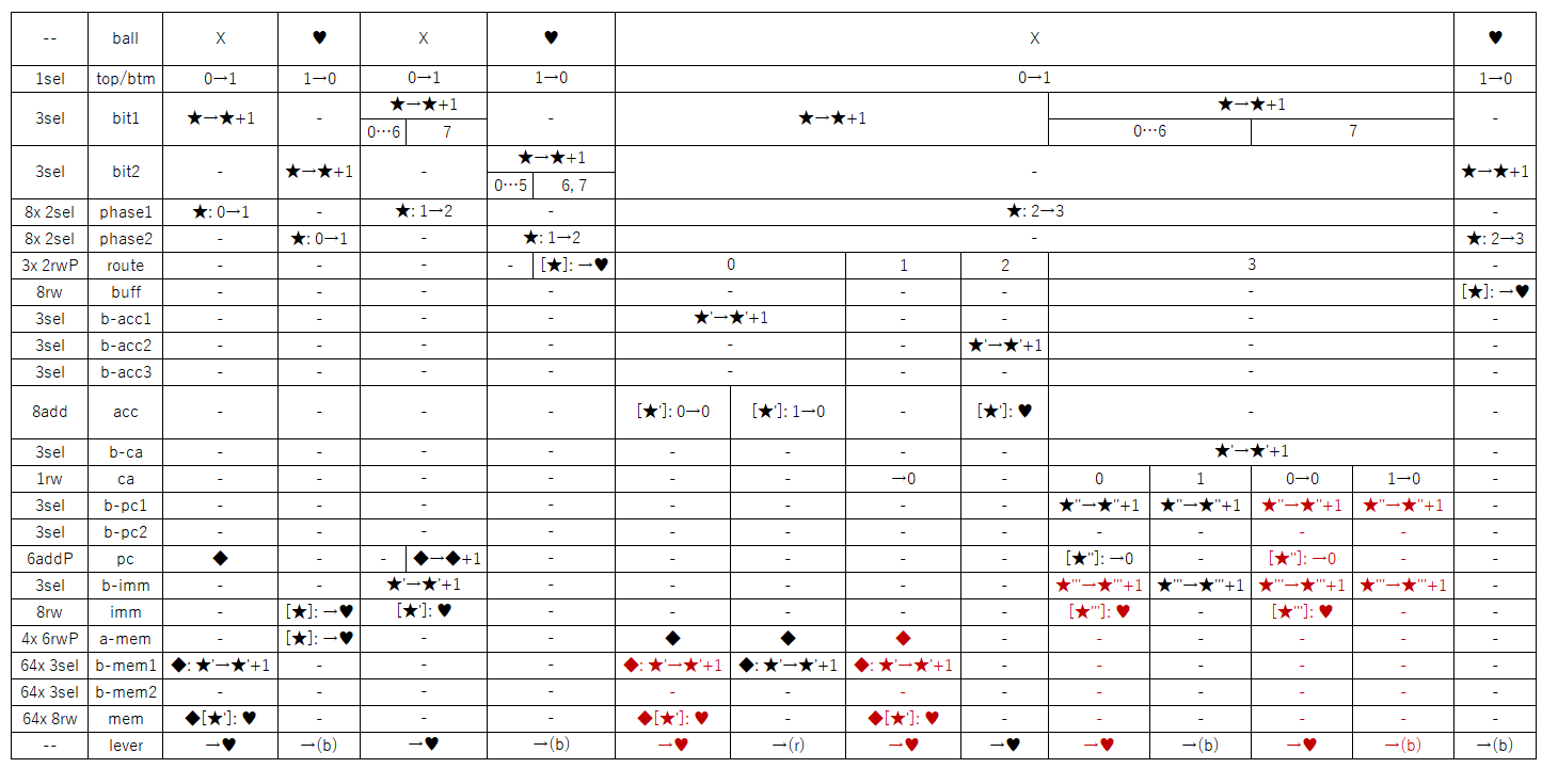
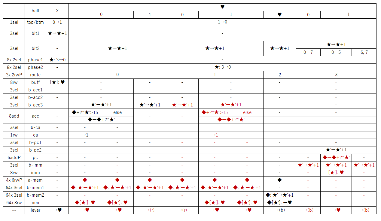
of that memory is the output of this sequence of events, and will be the color of the next ball.

The second ball will be in the next row.
Rewrite the corresponding bits of imm and a-mem according to :heart:, i.e., the color of the ball.

The following is a mathematical expression of the above.

imm = mem[pc]
a_mem = mem[pc]_6

“_6” means the lower 6 bits.

1 Like

After this, we can convert it into an expression in the same way

phase0

imm = mem[pc]
a_mem = mem[pc]_6

phase1

pc += 1
route = imm^2

phase2

route0:

acc = 0
buff = acc OR mem[a_mem]

route1:

ca = 0
buff = mem[a_mem]

route2:

buff = acc

route3: ca=0:

ca = 0
pc = 0
buff = imm

route3: ca=1:

ca = 0
buff = 0

phase3

route0:

{ca:acc} = {ca:acc} + NOT buff
// Here, the ca here doesn't change.

route1:

{ca:acc} = {ca:acc} + buff

route2:

mem[a_mem] = buff

route3:

pc += buff_6

The output of this, summarizing the four phases for each condition, is shown below.

route0(NOR) “00AAAAAA”

Accu = Accu NOR mem[AAAAAA]

route1(ADD) “01AAAAAA”

{ca:Accu} = Accu + mem[AAAAAA]

route2(STA) “10AAAAAA”

mem[AAAAAA] = Accu

route3(JCC) “11DDDDDD”

if(ca == 0)PC = DDDDDD
ca = 0

This is exactly the behavior of an MCPU.

As described above, a standard CPU could be built with TT.

That’s fantastic. What does it do?

This is incredible @Yama-chan! Now I can send this link to people who question it being a computer.

1 Like

How big a Turing Tumble board would one need to actually construct this?

This CPU has only 64 8-bit memories, so it cannot do anything complicated.
However, I think it can be programmed to perform four arithmetic operations between two digits.
The mcpu document(Listing 1, page 2) also shows an example of GCD calculation.

I made a rough guess.
The memory at the bottom [8rw] and the [6rwP] branching to it are going to be large.

Simply, the [8rw] is simply the height of 60 parts.
However, if we think about arranging 8 of these vertically and horizontally, it will be approximately 500 parts high.

For [6rwP], 63 sets of gear bit chains are needed to branch into 6bit=64.
This is also calculated to be about 500 parts high.
This is the same for [6rwP].

The other units are expected to be less than 100 high, so if we add these up, the total height will be less than 3000.
If we actually build it, it will be several tens of meters high and have tens of thousands of parts.

2 Likes